Semiconductor Research CenterFrom Materials to Optics: Building the Core Foundations of AI Applications
Faced with the challenges brought about by high-speed computing and data explosion in the AI era, Dr. Hao-Chung Kuo, Director of the Semiconductor Research Center, identifies three critical technologies as essential, energy-efficient enablers for AI data centers: compound semiconductors, silicon photonics, and nanophotonics.
From breakthrough research in gallium oxide (Ga₂O₃) semiconductors and high-speed silicon photonic chips to innovations in depth sensing and spatial computing, Taiwan continues to showcase its strength in advanced semiconductor development and intelligent sensing technologies.
Fourth-Generation Compound Semiconductors
Compared to conventional silicon, compound semiconductors such as silicon carbide (SiC) and gallium nitride (GaN) feature significantly wider bandgaps, almost three times that of silicon. This enables them to withstand higher voltages and temperatures, making them ideal for high-power electronics. Their wider bandgap also means electrons are less prone to scattering, which dramatically reduces leakage, enhances safety, and improves energy efficiency. Lower leakage translates to reduced energy loss, allowing for higher voltage and current output with less heat. Overall, power consumption can be cut by over 75%, and heat dissipation is up to three times more efficient than silicon.
Compound semiconductors were first used in electric vehicles, with Tesla pioneering their adoption as early as 2017. With the rapid development of AI, green energy, robotics, and drones, demand for applications that prioritize energy efficiency and extended battery life has surged, and compound semiconductors have thus become essential. In particular, integrating them into LLC converter circuits in AI servers can yield conversion efficiencies of up to 97 to 98%.
In August 2024, the Semiconductor Research Center, in collaboration with National Yang Ming Chiao Tung University (NYCU), achieved a major breakthrough in gallium oxide (Ga₂O₃) research. For the first time, the team successfully implemented P-type ion implantation and rapid thermal annealing on gallium oxide, followed by epitaxial growth of N-type and N+-type regions to form high quality homojunction structures. This enabled the fabrication of high-performance Ga₂O₃ PN diodes, marking a significant advance in fourth-generation compound semiconductor technology. The research was published in the prestigious journal Materials Today Advances.
With an ultra-wide bandgap of 4.8 eV and a breakdown field strength of 8 MV/cm, gallium oxide (Ga₂O₃) outperforms silicon, silicon carbide (SiC), and gallium nitride (GaN), making it a key material for high-voltage, high-temperature, and high-frequency applications. Japan, the U.S., and mainland China currently lead in gallium oxide research, but through the strategic collaboration with NYCU, Taiwan is rapidly closing the gap and is reinforcing its competitiveness in the global advanced semiconductor landscape.
Silicon Photonics: Breaking the Bandwidth Barrier
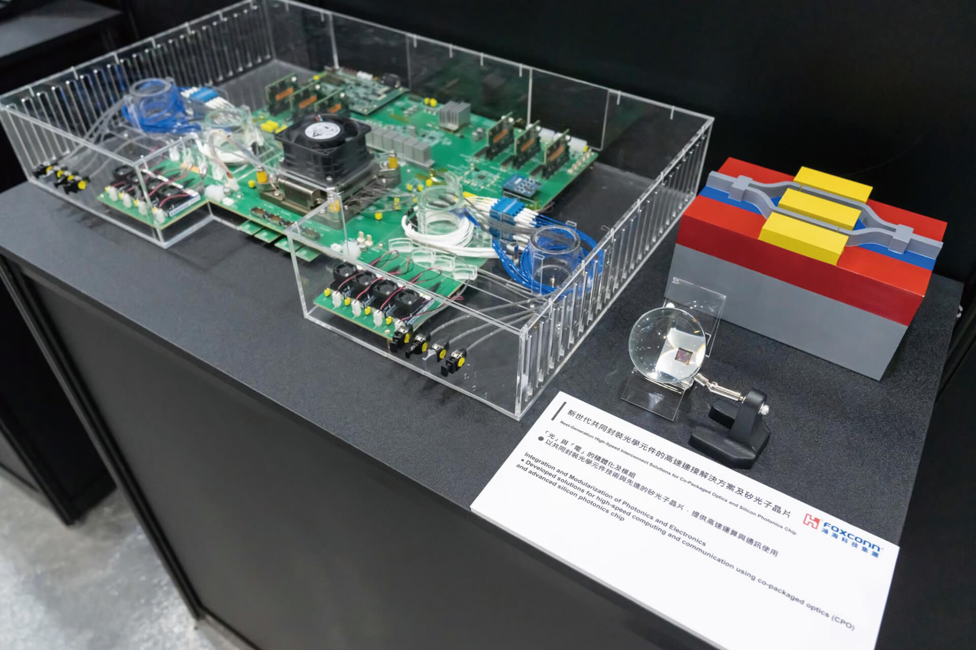
To address the mounting demand for high-speed data transfer and high bandwidth due to AI and data center expansion, HHRI has also invested in the development of silicon photonic chips.
Traditional optical systems are bulky and rely on discrete components. Silicon photonics, on the other hand, integrates the optical functions onto compact silicon chips to achieve a high degree of miniaturization. As AI has led to explosive demand for computing power and data throughput, the limitations of electrical signal transmission have become increasingly apparent, prompting a shift toward optical signaling. With chips now drastically miniaturized, there is no room for bulky optical systems alongside them, thus giving rise to the urgent need for integrated optical components.
The HHRI has designed critical components that integrate key optical elements onto silicon photonic chips. These include high-speed modulators that enhance single-channel transmission rates, on-chip photodetectors (PDs) that eliminate the need for external conversion back to electrical signals, and metasurface interface technology that embeds beam-deflecting lenses directly into the chip.
In parallel computing, silicon photonic chips enhance single-channel transmission speeds and long-distance signaling by converting electrical signals into optical signals for low-loss transmission via fiber optics. The process addresses the longstanding problem that “electrical signals don’t travel far.” By integrating complex optical components onto a single chip and expanding the number of usable wavelengths, silicon photonic chips enable multi-channel transmission and significantly increase the total bandwidth.
However, the pursuit of extreme miniaturization and high-speed transmission brings multiple challenges. Heterogeneous integration, which is integrating components of different materials and scales, poses a major engineering hurdle. Moreover, densely packing multiple components into a tiny space generates substantial heat, making both miniaturization and stability critical technical challenges.
In addition, the manufacturing and validation processes are both expensive and time-intensive. A single wafer run may cost millions of NT dollars, and design-to-validation cycles can span six months to a year. Furthermore, performing high-frequency measurements above 200 Gbps requires next-generation precision instruments, yet such capabilities remain limited in Taiwan. As a result, even well-designed chips might not be able to complete the full validation process.
“Our team moved swiftly. Design and tape-out were completed in just six months,” noted Dr. Hao-Chung Kuo. Despite formidable obstacles, silicon photonics research at HHRI has made significant strides, including the establishment of one of Taiwan's few laboratories capable of conducting 200 Gbps measurements. As a result, the team's siliconphotonics development remains globally competitive and, in certain areas, even ahead of its international counterparts.
Precision Light Control: Unlocking Miniaturization Potential
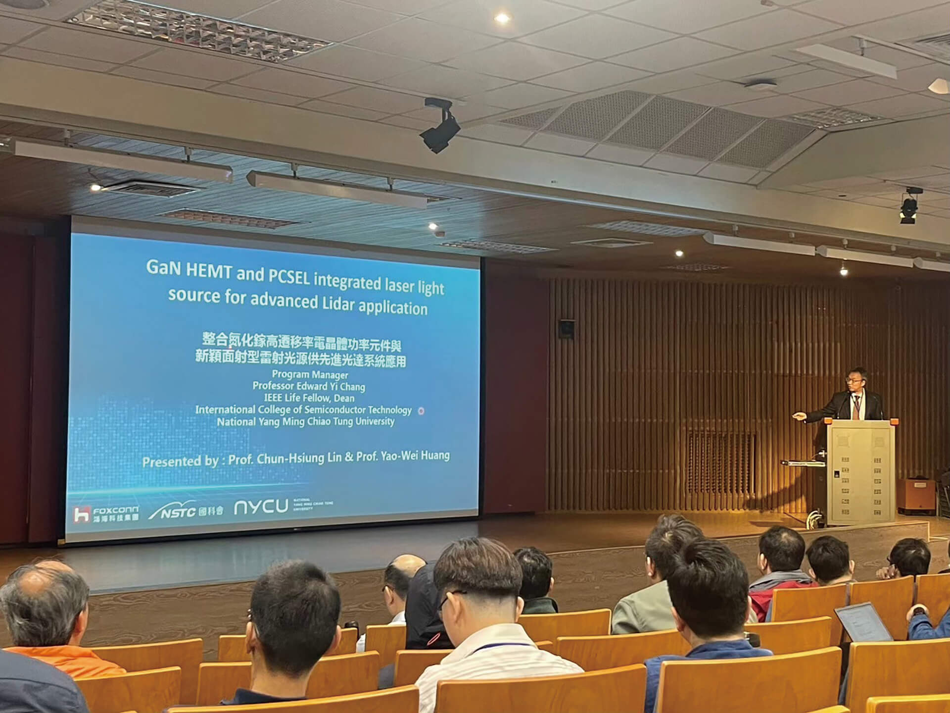
Beyond breakthroughs in Ga₂O₃ and silicon photonics, in 2024 the Semiconductor Research Center, in collaboration with NYCU, developed a novel depth-sensing and facial recognition system. This research was featured as the cover article of Nano Letters, a leading journal published by the American Chemical Society (ACS). It was also selected as a spotlight study in February 2024, accompanied by an exclusive interview. The work also received the Innovation Award at the 2024 I-Zone national smart display innovation showcase.
Built on depth sensing, the system determines the distance between an object and the camera lens by detecting variations in projected light points to reconstruct the object's shape and spatial position. The most widely known application is Apple's Face ID, which uses tens of thousands of infrared dots to generate a 3D contour of the user's face.
The research team used metasurface engineering to design and tune nanoscale structures on ultrathin films to precisely control the direction and focus of light. Previously requiring bulky lenses, these functions are now embedded into microchips, significantly reducing the size of optical modules while maintaining high customization and integration potential.
- Parallel Computing
- NVIDIA CEO Jensen Huang has pointed out that boosting computing power is no longer limited to chip-level miniaturization. Instead, the future lies in parallel, system-level computing, where multiple chips and boards work in concert to achieve exponential performance gains without pushing a single device to its limits.
In addition, this technology increases the number of sensing points, widens the field of view, and significantly reduces the size of the optical module from roughly one centimeter in an iPhone to a microchip just three human hairs wide, demonstrating exceptional miniaturization potential.
Additionally, it uses photonic crystal surface-emitting lasers and monocular stereo vision architectures, which simplifies device fabrication and enables monolithic integration. Take smartphone cameras as an example. Instead of separately fabricating and assembling multiple lenses and sensors, optical elements can now be embedded directly onto the chip, boosting both efficiency and reliability.
Driving the Next Generation of Spatial Computing
The novel depth-sensing and facial recognition system marks a major breakthrough in spatial computing. Apple's Vision Pro, for instance, relies on the real-time and accurate acquisition of depth information from the surrounding environment.
The technology developed by the HHRI–NYCU team lays the foundation for future depth-sensing applications, including AR/VR devices, drones, and smart vehicle systems. For instance, while the Apple Vision Pro contains as many as six built-in sensors, the ultracompact and lightweight nature of this technology allows AR/VR devices to become even smaller, more comfortable to wear, and far more energy-efficient.
For drone swarms of 50 to 100 units operating collaboratively, the technology facilitates efficient, precise point-to-point communication. Given drones’ strict constraints on component size and battery life, this technology enables longer battery life and higher payload capacity.
By improving performance at the hardware level, this technology reduces the burden on backend software, enabling sharper recognition and more efficient optical communication. Considered a next-generation functional light source, it optimizes system performance at the lowest level.
- Monolithic Integration
- Traditionally, nanoscale optical sensors were fabricated separately, lasers on one wafer, nanostructures on another, and then assembled later. Monolithic integration, by contrast, embeds nanoscale structures directly onto the laser chip, enabling the laser to emit a beam with specific properties and spatial profile at the point of light emission.